How to Make PCB on EasyEDA ?

What is PCB ?

A printed circuit board (PCB) mechanically supports and electrically connects electronic components using conductive tracks, pads and other features etched from copper sheets laminated onto a non-conductive substrate. PCBs can be single sided (one copper layer), double sided (two copper layers) or multi-layer (outer and inner layers). Multi-layer PCBs allow for much higher component density. Conductors on different layers are connected with plated-through holes called vias. Advanced PCBs may contain components – capacitors, resistors or active devices – embedded in the substrate.

The Process of Making a PCB Board ?

a. Start with a schematic

b. Layout PCB

c. Convert PCB File to Gerber File

d. Send to PCB Factory for sample production

1. Design Schematic , on EasyEDA , for example , design an Atmega16 simpliest system .

1.1 Create a Project . Document -New -Project

1.2 Create a Schematic and start designig a simplest system of MCU .

enter image description here

2. Make a PCB

2.1 Convert schematic to PCB and then Place the components in the proper position inside the Mechanical framework :

enter image description here

2.2 Start Routing a PCB manually .

2.2.1 Tips to Make PCB Circuit Board:

Sizing Traces

Real-world copper traces have resistance. This means that a trace has a voltage drop, power dissipation, and a temperature rise when current flows through it. Resistance is defined by this formula:

R=(resistivity∗length)(thickness∗width)

PCB designers most commonly use length, thickness, and width to control the resistance of a PCB trace. Resistance is a physical property of the metal used to make the trace. PCB designers can’t really change the physical properties of copper, so focus on the trace size, which you can control.

PCB trace thickness is measured in ounces of copper. One ounce of copper is the thickness we would measure if we evenly spread 1 oz of copper over a 1 square foot area. This thickness is 1.4 thousandths of an inch. Many PCB designers use 1 oz or 2 oz copper, but many PCB manufacturers can provide 6 oz thickness. Note that fine features like pins that are close together are hard to make in thick copper. Consult your PCB manufacturer about what their capabilities are.

Use a PCB trace width calculator to determine how thick and wide your traces should be for your application. Aim for a 5°C temperature rise. If you have extra space on the board, use bigger traces, as they don’t cost anything.

When doing a multi-layer board, remember that traces on external layers have better cooling than traces on internal layers because the heat from inner layers has to travel through layers of copper and PCB material before being conducted, radiated, or connected away.

Make Loops Small

Loops, especially high frequency loops, should be made as small as possible. Small loops have lower inductance and resistance. Placing loops over a ground plane further reduces inductance. Having small loops reduces high frequency voltage spikes caused by

V=Ldidt

. Small loops also help reduce the amount of signals that are inductively coupled into the node from external sources, or are broadcast from the node. This is what you want, unless you’re designing an antenna. Also keep loops small for op-amp circuits to prevent noise from being coupled into the circuit.

Decoupling Capacitor Placement

Place decoupling capacitors as near as possible to the power and ground pins of integrated circuits to maximize decoupling efficiency. Placing capacitors farther away introduces stray inductance. Multiple vias from the capacitor’s pin to a ground plane reduce inductance.

Kelving Connections

Kelvin connections are useful for measurements. Kelvin connections are made at the exact points to reduce stray resistance and inductance. For example, Kelvin connections for a current sense resistor are placed exactly at the resistor pads, not at some arbitrary place on the traces. Although on the schematic, placing the connections at the resistor pads or at some arbitrary point may look the same, real traces have inductance and resistance that could throw your measurements off if you don’t use.

Keep Digital and Noisy Traces Away from Analog Traces

Parallel traces or conductors form a capacitor. Placing traces close together capacitively couples the signals on the traces, especially if the signals are high frequency. Keep high frequency and noisy traces away from traces that you don’t want noise on.

Ground is not ground

Ground is not an ideal conductor. Take care to route noisy grounds away from signals that need to be quiet. Make ground traces large enough to carry the currents that will flow. Placing a ground plane directly under signal traces lowers the impedance of the traces, which is ideal.

Via Size and number

Vias have inductance and resistance. If you’re routing a trace from one side of the PCB to the other and need low inductance or resistance, use multiple vias. Large vias have lower resistance. This is especially useful in grounding filter capacitors and high current nodes.

Thermal vias

Vias can be used to move heat from one side of a PCB to the other. This is especially useful when a PCB is mounted on a heatsink on a chassis that can further dissipate heat. Large vias transfer heat more efficiently than small vias. Many vias transfer heat more efficiently than one via, and lower the operating temperature of components. Lower operating temperatures contribute to higher reliability.

Distances between traces and mouting holes.

Leave room between copper traces or fills and mounting holes; this helps prevent shock hazards. Solder mask isn’t considered a reliable insulator, so take care that there is distance between copper and any mounting hardware.

Heat sensitive components

Keep components that are sensitive to heat away from other components that generate heat. Examples of components that are sensitive to heat include thermocouples and electrolytic capacitors. Placing thermocouples close to heat sources may throw off temperature measurements. Placing electrolytic capacitors close to heat generating components will reduce their operating life. Components that generate heat may include bridge rectifiers, diodes, MOSFETs, inductors, and resistors. The heat depends on current flowing through the components.

Width of Trace :

The minimum width of trace is 4 mil when you layout very simple circuits ,and when you layout the current traces , you need to consider the width of Traces. Here with the relationship between the Trace width and the current .

Copper Thickness

35UM 50UM 70UM

Width Current Width Current Width Current

0.15 0.20 0.15 0.50 0.15 0.70

0.20 0.55 0.20 0.70 0.20 0.90

0.30 0.80 0.30 1.10 0.30 1.30

0.40 1.10 0.40 1.35 0.40 1.70

0.50 1.35 0.50 1.70 0.50 2.00

0.60 1.60 0.60 1.90 0.60 2.30

0.80 2.00 0.80 2.40 0.80 2.80

1.00 2.30 1.00 2.60 1.00 3.20

1.20 2.70 1.20 3.00 1.20 3.60

1.50 3.20 1.50 3.50 1.50 4.20

2.00 4.00 2.00 4.30 2.00 5.10

2.50 4.50 2.50 5.10 2.50 6.00

Laying out DC-DC voltage Circuits .

Laying out a DC-DC circuits , it should obey very strict rules according to the DC-DC Converter Datasheet .

Laying out High Speed Circuits and differential Circuits .

Laying out High-speed circuits also require designers to consider its impedance matching .And for the differential circuits we should parallel the wires and make impedance matching through a GND Layer or Power Layer. Every High-Frequency circuits requires impedance matching should be provided with a referential Layer .

Keep Noisy Circuits away from High-Speed Circuits

Noisy circuits too close to High-Speed circuits may cause the the High-Speed singal to distortion and affect normal operation of High-Speed circuits .

2.2.2 The Result of the MCU PCB Layout .

enter image description here

2.2.3 Pour the Copper on the BottomLayer .

enter image description here  https://easyeda.com/GerryChen/MCU_Project-HFzQ82kCU

3. Click the Photo view to check the Gerber file

enter image description here

4. Send Gerber file to PCB factory for PCB production and debug the the circuits by welding the components and ICs . That is a complete process of Making PCB board and Testing 、Debuging the circuits .

5. Easyeda Provides an cheap PCB Cart which offers low-price PCB and improve your efficiency to Make PCB .

Easyeda provides an Fabrication Output function . By clicking it , You can add the pcb order to cart and order the pcb board . You could wait at home or your company for the PCB and weld components at home or send to be welded by factory ,especially ICs with BGA Package .

Easyeda provides a one-stop shop for Electronics projects .You could go to it and experience designing Schematic & PCB and order PCB .

Source: https://easyeda.com/GerryChen/How_to_Make_PCB_on_Easyeda_-HFzQ82kCU

How to make PCB Layout On EasyEDA?

To draw PCB layout is an essential ability for electronic engineer .

We could use many tools for PCB Layout , Altium Designer, Kicad, PADS,and so forth .But for a reason that these software are all desktop-based , you need to install it on your PC or may need to pay for the software .EasyEDA provides a feasible way to draw schematic and PCB online ,without installing a software on your PC , and you could also save it on the cloud server and share it to all the internet users in the meantime .You could utilize all the internet components Lib and PCB Lib on the internet , you could edit the Libs and add them to your Part. You could also utilize the accomplished module in the System Design or the User’s Design. That really accelerates your speed to accomplish a Project . Furthermore, you could add the PCB Layout to Your CART and pay for it with low cost for the PCB order . That is an easy way to accomplish your Project from Concept Design ,Schematic Design to PCB Design and PCB order .

Let me introduce how to make PCB Layout out of an online schematic design on EasyEDA , an free online schematic design Tool ,spice simulation tool, PCB Design tool .

We need to Firstly create a Schematic .

Let us create e a DC/DC Converter schematic as followed.

schematic design

https://easyeda.com/GerryChen/LM2596_Module__Adjustable_DC_DC_Power_Converter_1_25V_35V_3A-4y4YgarJD


The schematic consists of a power management IC LM2596s-ADJ ,A DC-DC Step-Down Power IC

A feedback circuit including R2&R1 ,a resistor R2 and an adjustable resistor R1 , Vin and Vout Filter Capacitor C1&C2. A led Indicator circuit of output.

Choose package for every component .

Then convert the schematic into PCB by clicking “Convert To PCB ”ICON on the Toolbar.

Then it will transfer to New PCB file

Press”Ctrl+S” to save the New PCB and rename it .

On the external frame , click the arc and delete it . Close the external frame with right angle .

PCB file

——Change the arc on the left top side to right angle .


Click every component and drag them to the inside of the frame .

Put every component on the proper position .

Then start to route it as followed .

1、Auto route

2、Route manually .

1、You could choose to auto route the circuit by clicking the auto route .

After clicking “Auto Router” ICON ,the interface will pop up with Auto Router Config .You could modify the track width , General clearance ,and so on .Click run to execute auto routing .

auto route PCB layout

——Auto Router Config dialog.


PCB layout

——Effect of Auto Routing .

2、However , even the tool provides function to auto route, for most of the completed circuits or special circuits , you need to route it manually .

3、Use the PCB tools and the layers tools and use the track on the PCB Tool to connect every flying line .

4、Remember to check the DRC Routing Rule and then make the PCB Layout to make sure that it support power integrity .After you route the wire , change the size of Toplayer Silklayer .

5、Pour the Copper Area through the icon PCB toolon the PCB tool.

6、Press ”M” or click the “Dimension ”ICON PCB toolon the PCB tool to measure the width and the length of the PCB board.

PCB layout

https://easyeda.com/GerryChen/LM2596_Module__Adjustable_DC_DC_Power_Converter_1_25V_35V_3A-4y4YgarJD

——Result of manual routing and measure the width or length of the circuit board .

7、Commonly we pour copper on the bottom layer as ground network ,pour the copper to the Top layer as the power network .

8、After you have route the PCB ,you could click the Designer Manager on the right hand side .

9、Then it will transfer to Properties .Click DRC Errors and Refresh .There are no DRC Errors in the PCB Layout .Click the components and nets , you could make every components or net bright. For example , choose C2 and The capacitor C2 will become bright .

10、Let us manually make an error . For Example , move MDC wire and there will be a big bright X and DRC Errors track2pad error.

PCB layout

Move the track to its previous location and then then big X and the DRC errors will disappear.

Once you have finished the PCB Layout , Click photo view to produce the Gerber file .

PCB layout

——PCB photo preview


11、If you want to order the PCB board ,Click the Fabrication Output icon in the Toolbar to order the PCB ,Then go to the Add to Cart Interface .

There are items like Numbers of Layers ,PCB Dimension Width and Height ,PCB Thickness ,PCBQTY,PCB Color,Surface Finish ,Copper Weight ,And Penalized PCB .

When you fill in all the Items above ,save it to cart. Then go the Network Payment Interface .

Delete the useless Gerber file .

Fill in your country ,your name ,your address ,your Post/Zip Code ,your Telephone ,Choose Delivery Method ,Network Payment Items ,and Click to send Request .

PCB order

OK , then just wait for your PCB Order at home .

How to make online PCB Design

It sounds great to make an online PCB Design and share with all the people and also you could edit Online PCB .
Do you think it is great ? There are some online Circuit Designer ,for example , circuitlab , upverter and easyeda .
For there are no PCB layout function on Circuit Lab ,and I need to register an account on Upverter so I could start to design , and EasyEDA can be used without registering.so I choose to experience EasyEDA.
Just open https://easyeda.com/.I have tried it without registering at first. I found it’s easy to use and just what I need.So I registered.and certainly registering an account will provides us much more functions , that will help you a lot in designing circuits ,saving your projects on the cloud sever and sharing with friends or colleagues.Let us look at the Register and Login interface first .
  ——The Register and Login Interface .
Then create a new Project:
Check what are there on the website main page .
  ——The mainpage of https://easyeda.com/
Click New Project and we can go to the Editor :https://easyeda.com/editor
  ——The diagram of the Editor
On the Editor Interface, there are Toolbar, Schematic,Design Manager, Wiring Tools ,Drawing Tools,Preview. And on the left size there are items like My Projects, My Parts, Shared with me,Favorite Parts, EasyEDA Libs &General Package.
Let me introduce How to draw a schematic now .
For example , draw a LED Light Circuit. You could choose the component on the left-hand side :Using easyeda Libs ,click to put a resistor , a led Light , a power source ,a ground ,a capacitor . Then connect them into a circuit with wire in wiring Tools.The color of the Schematic background , the color of the wire or the text , or the Netlist ICON and so forth can be changed in colors. OK ,let us See the completed schematic .
  ——A Led Light Schematic Example .
Then choose package for every component , the resistor 0603 package, the LED 3MM,the capacitor choose 0805 package.
Click the component ,then go to the design Manager, then click the space in the package , then it will come out with the dialog of “Update the symbols’ Package”Then choose the package in the user package ,favorite Package ,or general Package .Or input the package name in the space if you know package name in your parts your favorite parts or in the system package .

You could also preview the package of the components. For instance , choosing an 0805 package for a capacitor .
  ——Choose the Package for the component and preview.
Then you could easily know whether the component is suitable for your design.
You could also drag the update component package and preview Tool to proper position as you expect.
Then convert the schematic to PCB .
About How to convert Schematic to PCB , Please refer to File “How to convert Schematic to PCB”.
For most of the simple circuits , you could choose auto route to layout the PCB .Thanks to hardworking of EasyEDA team ,the EasyEDA could do online PCB auto routing .It feels wonderful and convenient to route simple one-or-two layer boards .
Check the effect of auto routing .
  ——The effect of Auto Routing1
It seems so simple that I could not be brave enough to put it in online ,but it is just used to illustrate what it is like when auto routing very simple circuits.
Let me show another complex auto routing effect diagram:https://easyeda.com/GerryChen/MQ5_Se…ject-F1VdvpGYg
  ——The Effect of Auto Routing2.
  ——The Effect of Photo Preview
Then you could have a photo preview to check whether the Layout can be used in real Product .
For More complex Project , you could also choose auto routing . You could just slightly adjust the Routing .
Even though it could auto route, I think for most of complex projects ,we should route the PCB manually .
In summary , I feel it provides us with much convenience to build small-scale or middle-scale projects anywhere accessible to Internet . I need not to install an EDA software on my PC ,neither do I need to create most of the Schematic Lib or PCB Lib personally .I need not to just use the Design of myself , I could also apply some online electronic designs from electronic freaks or engineers , no matter you are beginners or professional engineers , I could learn knowledge from your design, I can get inspiration from your simple designs or complex designs, from your industrialized designs or just the designs out of your hobbies . Sometimes, if I want to create a Project ,I could use most of the Sample Designs ,most of the Online Schematic Lib or PCB Lib. If there is not Lib I wanted , I could build one online and it could be shared with all the Online Designers. I feel it is not just saving most of my time on Design, but also provides convenience to all the online Designers .There are fulfillment when I finish many SCH Lib or PCB Lib or One Complete Project and they would possibly be adopted.

Electrical circuit design and simulation online By using EsayEDA

Today, I used the EasyEDA online software, to my surprise for the optimization of the interface.There’s nothing more than anything. And then look at the EasyEDA tool seriously, not only the design of the schematic diagram, but also powerful PCB rendering capabilities. Before it, we use the EDA software has a lot of modules are charged, and many electronic circuit simulators are also charged. But the electronic circuit simulator of EasyEDA is free of charge, this saves us a lot of time and money.It is more conducive to our design of the circuit.
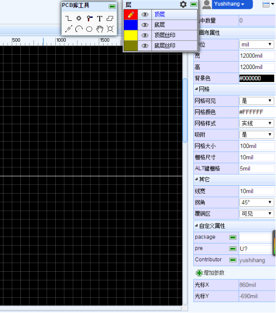
PCB tools
The drawing of PCB is one of the things that make us worry,especially when there is no thought. The interface is very friendly. The two toolbars can be very easily suspended for coloring on the original device, and the right side of the toolbar of the background color, the color of the grid, the grid size, grid format and other modifications can be modified.As shown :

Electronic circuit simulation
I plan to design a single amplifier circuit, and the simulation of it. First of all I want to find all the components in the toolbar on the left,such as Power, resistance, inductance,an so on. The left toolbar contains most of our usual design commonly used circuit device, and it’s easy to find them.And there are many examples you can refer to if you have any difficulty when you draw a schematic,just searching at here https://easyeda.com/example
This is different from other simulation software, other simulation software is in the form of drag and drop, but this software is in the form of click. It makes us more relaxed. After the original device is found, we will carry out the construction of the schematic diagram..As shown

  Electrical circuit simulator online

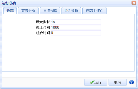
Finally, the software is used to simulate the online simulator.I find maximum step length, termination time, starting time, AC analysis, DC scanning can be set and modified, the shortage is that the lack of settings that can modify the last emulator. As shown

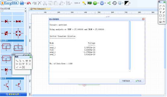
The result of simulation as shown

  EasyEDA has good simulation support using ngspice. Many LTspice simulations can be run in ngspice with little editing effort.

How to use EasyEDA draw a easy schematic diagram

Eagle schematic editor
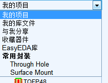
The same as the others electronics circuit drawing software,at the top of EasyEDA is the main toolbar,under the main toolbar,there are three parts, the lift part are projects associated with user, such as My Project,My library,EasyEDA library,Common Package and so on.Selecting one, you can view the corresponding subfolders.Generally,Switching to EasyEDA library, the common components can be found here, which is convenient for drawing.https://easyeda.com/editor
EasyEDA
The middle part is the canvas,the drawing area.
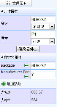
You can find the manager for the design and the attribute information of component at the right hand of the canvas.Selecting the components,you can modify package and Manufacturer that are the device information and the custom properties .
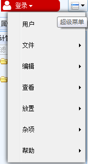
The most unique of EasyEDA is that provided with the super menu,Expanding the small triangle on the top right corner,you can see the contents shown below,all the essential tool can be found here.
 Some preparatory works before draw circuits
Before drawing a circuits,some components you need should be found.Unlike the Protel 99se,the components search interface of EasyEDA is very simple,and easy to use.Typing a Search keyword, the desired components can be found.Specifically as follows.
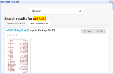
Left-click the More libraries,typing in the search bar to look for a component,for example,At89C51 is the retrieved component,the search results are shown below,the results have two categories,which are System Component and User Component.There are same different types of 89 series of microcontrollers.The user can choose the type of microcontroller according to their own requirements.
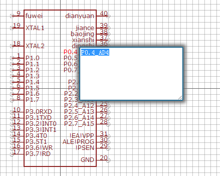
  Lift-clicking Place,in the schematic, click the left mouse button,the components can be placed into the schematic interface,Right-clicking and ending component placement.Clicking Edit and entering the editing interface,you can modify the component’s pin number and name.Double clicking the left mouse button to modify the pin and typing custom name.Taking AT89C51 as an example,RES is replaced by fuwei,VCC is changed into dianyuan.As the picture shown below,customizing the Pin Name,which makes its reader easier to understand , and moreover makes its user easier to use.
schematic diagram

Online schematic diagram maker—EasyEDA

Traditional EDA tools/software facilitates our electronic design, they are powerful and convenient. However, in the time of makers,they’re not satisfied with the desktop tools. If you work on different workstations, or uses different operation systems, updating your data between two computers brings a problem. But with online EDA tools, there is nothing to worry about.

Few weeks ago, I found a cloud based EDA tool, EasyEDA. Not like other online EDA tools, it’s free for us. Cloud makes it compatible across different device or operation systems. You can design circuit, PCB layout, run simulation or analysis with EasyEDA. Wherever you are, you just connect to Internet and open your browser, then start your work. You can take a break and upload it to the cloud. The next time you want to continue, just login into the website. It provides over 70,000 readily available schematic and over 15,000 PSpice libraries in their database, which makes it no less than those traditional EDA desktop tools.

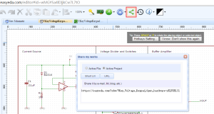
But a cloud based tool is not just convenient for mobility. What’s more, it allows you to share production or performance with friends and workmates on the cloud. It provides an URL code of your projection. With the address, you could share it on Facebook, Twitter and Google+ or by email. So you can communicate with your team more conveniently, which will greatly improve the efficiency of your projection. As a greenhorn in maker,I found it really helped me a lot. I joined a project online, team members come from everywhere. So mostly we communicate through email and Twitter. EasyEDA makes sharing project convenient for us. We send the address of project and the other person could read and edit it on webpage. This makes our teamwork efficient.

What really interests me is that you can order PCB on EasyEDA. You design it, and the website contact factory to product. Because of the large number of users and orders, every single PCB does not cost us much. I used to look for a factory to print the PCB that I designed, that spenda lot of time and money. Now I got EasyEDA, I could save a lot. (^o^)

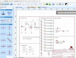
Here is one of my work made in Easyeda,and you can have a try on http://easyeda.com/editor too.

my work on EasyEDA
my work on EasyEDA

After you finished your design,you can easily share it to others.

图片2